PCB fabrication
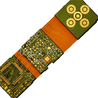
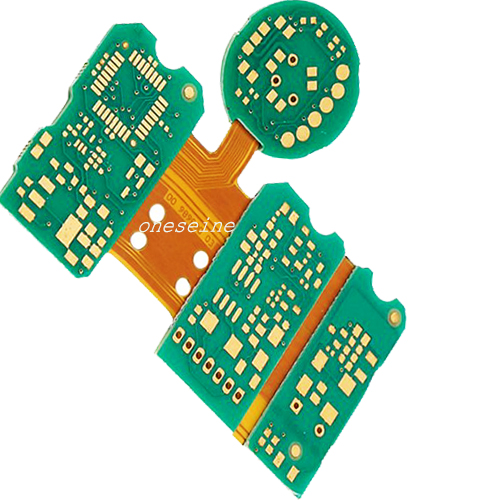
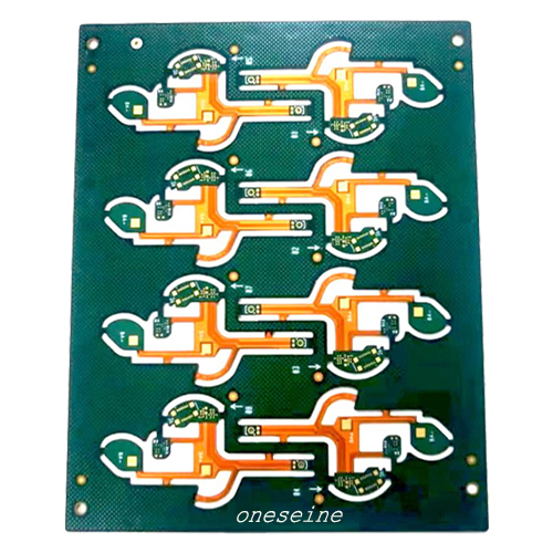
4 Layer Multilayer PCB 1.6mm Thickness Integrated Circuit Board
4 Layer Multilayer PCB 1.6mm Thickness Integrated Circuit Board
Specification:
Base Material: Fr4 KB Material and prepreg |
Layer:4 |
Thickness: 1.2MM |
Copper weight:1OZ |
Surface finish: HASL LF |
Core: 2 |
Name: Multilayer PCB |
4 Layer Multilayer PCB Prototype,4 Layer PCB Fabrication,4 Layer PCB Manufacturer in China |
4 Layer Multilayer PCB Maker, Fast delivery time |
4 Layer PCB fabrication process:
Chemical clean
In order to obtain good quality etched patterns, it is necessary to ensure that the resist layer is firmly bonded to the substrate surface, requiring no oxide, oil, dust, fingerprints, and other dirt on the substrate surface. Therefore, before the application of the first layer of the surface of the plate to be cleaned and copper foil surface to a certain degree of coarsening.
Inner plate: start to do four layers, the inner layer (the second layer and the third layer) is to be done first. The inner sheet is a copper sheet laminated on the upper and lower surfaces by a glass fiber and an epoxy resin base.
Cut sheet ,dry film lamination:
Photoresist: To make the desired shape in the inner layer, we first apply a dry film (photoresist, photoresist) to the inner layer. Dry film is made of polyester film, photoresist film and polyethylene protective film composed of three parts. When the film, first from the dry film peeling off the polyethylene protective film, and then under the conditions of heating and pressing the dry film paste on the copper surface.
Image exposure:
Exposure: Under the irradiation of ultraviolet light, the photoinitiator absorbs the light energy to decompose into free radicals. The free radicals then cause the photopolymerization monomer to produce polymerization cross-linking reaction. After reaction, it forms polymer structure insoluble in dilute alkali solution. Polymerization reaction will continue for some time, in order to ensure the stability of the process, not immediately after exposure to tear polyester film, should stay more than 15 minutes to when the polymerization reaction continues, tearing polyester film before development.
Development: the photosensitive film in the unexposed part of the active groups and dilute alkali solution reaction soluble soluble and dissolved down, leaving the photosensitive cross-linked curing part of the graphics.
Etching:
In the flexible printed circuit board or printed circuit board production process, the chemical reaction method will not be part of the copper foil to be removed, so that the formation of the required circuit pattern, photoresist below the copper is preserved from etching The impact of.
Strip resist,post etch punch,AOI inspection,Oxide:
The purpose of the film removal is to remove the resist layer remaining on the etched back so that the underlying copper foil is exposed. "Membrane residue" filtration and waste recovery should be properly handled. If the washing to the membrane can be completely cleaned, you can consider not pickling. After the final cleaning board to be completely dry to avoid water residue.
Layup with prepreg
Before laminating press, the raw materials should be prepared for the lay-up operation, except for the oxidized inner layer, the protective film (Prepreg) - Epoxy resin impregnated glass fiber. The function of the laminations is to laminate the sheets covered with the protective film in a certain order and place them between the two steel sheets.
Layerup with copper foil,Vacuum lamination press
Copper foil - to the current inner plate and then on both sides are covered with a layer of copper foil, and then multi-layer pressure (in a fixed time need to measure the temperature and pressure extrusion) After cooling to room temperature, the remaining Is a multi-layer together the laminate.
CNC drill:
In the inner layer of accurate conditions, the NC drilling according to the mode of drilling. Drilling accuracy is high to ensure that the hole is in the correct position.
Electroplating copper
In order for the vias to be conductive between the layers (metallization of the resin and glass fiber bundles on the non-conductor portion of the cell walls), the pores must be filled with copper. The first step is a thin layer of copper plated in the hole, the process is completely chemical reaction. The final thickness of copper plated is 50 parts per million.
Solder mask
Surface finish
Profile
Testing
QC Inspection
Package
4 Layer Multilayer PCB parameter:
Number of Layer | 4 Layer |
Order Quantity | 1 to 50,000 |
Board Shape | Retangular,round,slots,cutouts,complex,irregular |
Board Type | Rigid, Flexible, Rigid-flexible |
Board Material | FR-4 glass epoxy, FR-4 high Tg, Rohs compliant,Aluminum,Rogers,etc. |
Board Cutting | Shear,V-score,Tab-routed |
Board Thickness | 0.2-4.0mm, Flex 0.01-0.25mm |
Copper Weight | 1.0, 1.5, 2.0 ,3.0,4OZ |
Solder Mask | Double-sided green LPI,Also support Red,White,Yellow,Blue,Black |
Silk Screen | Double-sided or single-sided in white,yellow,black,or negative |
Silk Screen Min Line Width | 0.006'' or 0.15mm |
Max Board Dimensions | 20 inch*20inch or 500mm*500mm |
Min Trace/Gap | 0.10mm, or 4mils |
Min Drill Hole Diameter | 0.01'',0.25mm, or 10mils |
Surface Finish | HASL,Nickle,Immersion Gold,Immersion Tin,Immersion Silver,OSP,etc. |
Board Thickness Tolerance | ±10% |
Copper Weight Tolerance | ± 0.25 oz |
Minimal Slot Width | 0.12'', 3.0mm, or 120mils |
V-Score Depth | 20-25% of board thickness |
Design File Formate | Gerber RS-274,274D,Eagle and AutoCAD's DXF,DWG |
Categories
News
Contact Us
Contact: Flexible PCB
Phone: 0086 18682010757
E-mail: kico@oneseine.com
Add: Building9,Xinyuan Industrial Park,Tangwei,Fuyong,Baoan,Shenzhen,China


