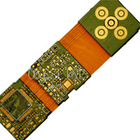
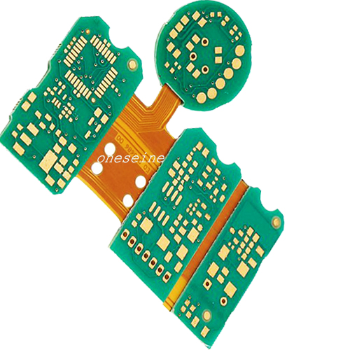
Rigid-flex FPC
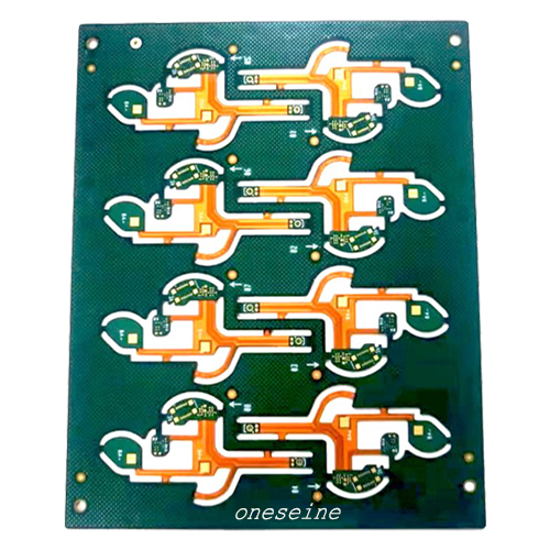
1oz FR4 Rigid Polyimide Flexible Circuit PCB 8 Layers PCB 1mm Green Cover Film
1oz FR4 Rigid Polyimide Flexible Circuit PCB 8 Layers PCB 1mm Green Cover Film
Product Introduction
Brand:oneseine
Number of layers: 8
Material: Shengyi TG170-S1000
Plate thickness: 2.0 ± 0.1mm
Minimum aperture: 0.15mm
Minimum line width/line spacing: 0.08mm
Copper thickness: 1OZ each on the inner and outer layers
Solder resistance: green oil with white letters
Surface technology: sinking gold
Product features: 0.1mm hole to line, 0.2mm BGA pad, resin plug required for holes in the pad
Oneseine with 15 years of professional technical experience-
With over 16 years of experience manufacturing flexible PCBs for the automotive industry, oneseine is proud to provide high-quality, reliable solutions for battery protection circuit boards.
Our 2-layer flexible PCB is specially designed for automotive new energy applications, providing a durable and efficient solution for battery protection. Our flexible PCBs are made of high-quality materials such as PI, copper and adhesives to meet the needs of automotive use. A plate thickness of 0.25mm +/- 0.03mm ensures a strong, reliable construction, while a minimum hole size of 0.1mm ensures precision and accuracy in assembly.
Our flexible PCBs are designed with 0.2mm/0.25mm line width and space to provide superior performance and functionality. ENIG 2-3uin's surface treatment provides a corrosion-resistant surface ensuring long-lasting durability and reliability in automotive applications. With a tolerance of ±0.1mm, our flexible PCBs are guaranteed to meet the exact specifications and requirements of your battery protection circuit board.
At oneseine, we understand the critical importance of quality and reliability in automotive applications. That’s why our Automotive New Energy 2-Layer Flexible PCB – Battery Protection Circuit Board is engineered to meet the highest performance and durability standards. With our extensive experience in manufacturing flexible PCBs for the automotive industry, we have the technical expertise and knowledge to provide high-quality products that meet the unique needs of new energy applications.
Whether you are looking for solutions for electric vehicles, hybrid vehicles, or other new energy vehicle applications, Oneseine's 2-layer flex PCBs are ideal for your battery protection circuit board needs. Our commitment to excellence and innovation ensures you will receive quality products that meet and exceed your expectations.
Oneseine is a brand you can trust when it comes to manufacturing flexible PCBs for automotive new energy applications. Our dedication to quality, reliability and technical excellence has made us an industry leader. With our 2-layer flexible PCB for automotive new energy – battery protection circuit board, you can be confident in the performance and durability of your battery protection system.
Choose Oneseine for your flexible PCB needs and experience the difference our expertise and commitment to quality make. Contact us today to learn more about our 2-layer flexible PCB – battery protection circuit board for automotive new energy and learn how we can meet your unique specifications and requirements.
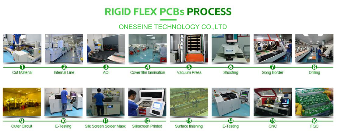
Rigid flexible Circuit Board PCB Fabrication Process:
1. Cutting: Cutting of hard board base material: Cut a large area of copper-clad board into the size required by the design.
2. Cutting the flexible board base material: Cut the original roll material (base material, pure glue, covering film, PI reinforcement, etc.) into the size required by the engineering design.
3. Drilling: Drill through holes for circuit connections.
4. Black hole: Use potion to make the toner adhere to the hole wall, which plays a good role in connection and conduction.
5. Copper plating: Plate a layer of copper in the hole to achieve conduction.
6. Alignment exposure: Align the film (negative) under the corresponding hole position where the dry film has been pasted to ensure that the film pattern can correctly overlap with the board surface. The film pattern is transferred to the dry film on the board surface through the principle of light imaging.
7. Development: Use potassium carbonate or sodium carbonate to develop the dry film in the unexposed areas of the circuit pattern, leaving the dry film pattern in the exposed area.
8. Etching: After the circuit pattern is developed, the exposed area of the copper surface is etched away by the etching solution, leaving the pattern covered by the dry film.
9. AOI: Automatic optical inspection. Through the principle of optical reflection, the image is transmitted to the equipment for processing, and compared with the set data, the open and short circuit problems of the line are detected.
10. Lamination: Cover the copper foil circuit with an upper protective film to prevent circuit oxidation or short circuit, and at the same time function as insulation and product bending.
11. Laminating CV: Press the pre-laminated covering film and reinforced plate into a whole through high temperature and high pressure.
12. Punch: Use the mold and the power of the mechanical punch to punch the work plate into the shipping size that meets the customer's production requirements.
13. Lamination (superposition of rigid-flex pcb boards)
14. Pressing: Under vacuum conditions, the product is gradually heated, and the soft board and hard board are pressed together through hot pressing.
15. Secondary drilling: Drill the via hole connecting the soft board and the hard board.
16. Plasma cleaning: Use plasma to achieve effects that conventional cleaning methods cannot achieve.
17. Immersed copper (hard board): A layer of copper is plated in the hole to achieve conduction.
18. Copper plating (hard board): Use electroplating to thicken the thickness of hole copper and surface copper.
19. Circuit (dry film): Paste a layer of photosensitive material on the surface of the copper-plated plate to serve as a film for pattern transfer. Etching AOI wiring: Etching away all the copper surface except the circuit pattern, etching out the required pattern.
20. Solder mask (silk screen): Cover all lines and copper surfaces to protect the lines and insulate.
21. Solder mask (exposure): The ink undergoes photopolymerization, and the ink in the screen printing area remains on the board surface and solidifies.
22. Laser uncovering: Use a laser cutting machine to perform a specific degree of laser cutting on the position of the rigid-flex junction lines, peel off theflexible board part, and expose the soft board part.
23. Assembly: Paste steel sheets or reinforcements on the corresponding areas of the board surface to bond and increase the hardness of important parts of the FPC.
24. Test: Use probes to test whether there are open/short circuit defects to ensure product functionality.
25. Characters: Print marking symbols on the board to facilitate the assembly and identification of subsequent products.
26. Gong plate: Use CNC machine tools to mill out the required shape according to customer requirements.
27. FQC: The finished products will be fully inspected for appearance according to customer requirements, and defective products will be picked out to ensure product quality.
28. Packaging: The boards that have passed the full inspection will be packed according to customer requirements and shipped to the warehouse
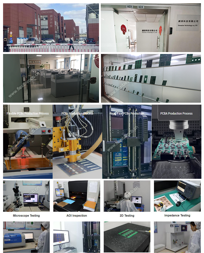
Oneseine Flexible PCB & Rigid-Flex PCB Process Capability
| Category | Process Capability | Category | Process Capability |
| Production Type | Single layer FPC / Double layers FPC Multi-layer FPC / Aluminum PCBs Rigid-Flex PCB | Layers Number | 1-30 layers FPC 2-32 layers Rigid-FlexPCB 1-60 layers Rigid PCB HDI Boards |
| Max Manufacture Size | Single layer FPC 4000mm Double layers FPC 1200mm Multi-layers FPC 750mm Rigid-Flex PCB 750mm | Insulating Layer Thickness | 27.5um /37.5/ 50um /65/ 75um / 100um / 125um / 150um |
| Board Thickness | FPC 0.06mm - 0.4mm Rigid-Flex PCB 0.25 - 6.0mm | Tolerance of PTH Size | ±0.075mm |
| Surface Finish | Immersion Gold/Immersion Silver/Gold Plating/Tin Plating/OSP | Stiffener | FR4 / PI / PET / SUS / PSA/Alu |
| Semicircle Orifice Size | Min 0.4mm | Min Line Space/ width | 0.045mm/0.045mm |
| Thickness Tolerance | ±0.03mm | Impedance | 50Ω-120Ω |
| Copper Foil Thickness | 9um/12um / 18um / 35um 70um/100um | Impedance Controlled Tolerance | ±10% |
Tolerance of NPTH Size | ±0.05mm | The Min Flush Width | 0.80mm |
| Min Via Hole | 0.1mm | Implement Standard | GB / IPC-650 / IPC-6012 / IPC-6013II / IPC-6013III |
News
Contact Us
Contact: Flexible PCB
Phone: 0086 18682010757
E-mail: kico@oneseine.com
Add: BldB,Fushan Industrial Park,Qianwu Town,Doumen,Zhuhai,China
