PCB fabrication
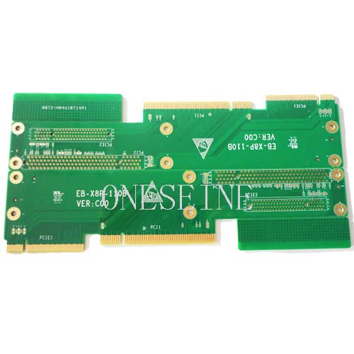
Multilayer Fr4 Industrial Control System Turnkey PCB Board
Multilayer Fr4 Industrial Control System Turnkey PCB Board
PCB Quick detail:
Layer: 4 layers
Finished thickness: 2.6mm
Min outer layer line width / distance: 0.1mm/0.11mm
Min inner layer line width / distance: 0.12mm/0.15mm
Min aperture: 0.25mm
Minimum BGA solder joint: 0.23mm
Impedance requirements: 50 ohm, Tolerance + / -10%
Surface finished: Immersion Gold
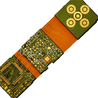
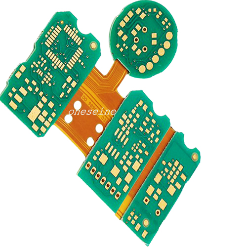
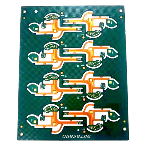
Industrial Control PCB:
Are you looking for design help with your Industrial Control PCB or Printed Circuit Board project? Oneseine has emerged as a leading PCBA manufacturer of time-critical, high performance Industrial Control PCB, Industrial Control PCB Board, printed circuit board solutions.
Industrial Control PCB Board Specifications
High quality Industrial Control Board
-PCB & PCBA Service
-UL,SGS,Rohs Certificated
-Competitive Price,High Quality
Our Capabilities of Industrial Control PCB Manufacturing
Total Pad Size | Standard | Advanced |
Capture Pad | Drill + 0.008 | Drill + 0.006 |
Landing Pad | Drill + 0.008 | Drill + 0.006 |
BC Mechanical Drill (Type III) | 0.008 | 0.006 |
Laser Drill Size | 0.004-0.010 | 0.0025 |
Material Thickness | 0.0035 | 0.0025 |
Stacked Via | Yes | Yes |
Type I Capabilities single & Double Deep | Yes | Yes |
Type II Capabilities Buried Vias with Microvias | Yes | Yes |
Type III Capabilities | Yes | Yes |
Copper Filled Microvia | Yes | Yes |
Smallest Copper Filled Microvia | 0.004 | 0.0025 |
Copper Filled Microvia Aspect Ratio | 0.75:1 | 1:1 |
Smallest Laser Microvia Hole Size | 0.004 | 0.0025 |
Laser Via Aspect Ratio (Depth:Diameter) | 0.75:1 | 1:1 |
Categories
News
Contact Us
Contact: Flexible PCB
Phone: 0086 18682010757
E-mail: kico@oneseine.com
Add: BldB,Fushan Industrial Park,Qianwu Town,Doumen,Zhuhai,China
