PCB fabrication
Step Copper PCB Circuit Boards With External layers has a Combination of the standard(4OZ) and Heavy /EXTREME(30oz) Copper
Step Copper PCB Circuit Boards With External layers has a Combination of the standard(4OZ) and Heavy /EXTREME(30oz) Copper
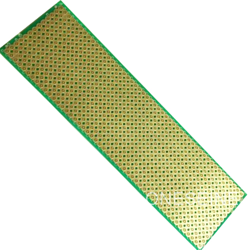
PCB boards Spec:
Board size:20*5CM
Material:Fr4
Special:Heavy copper
Copper weight:4OZ and 30OZ
Questions:
1. what is the maximum copper weight that you can cater?
30OZ
2. Are there special notes that should be declared on the FAB note instructions? (e.g. minimum trace width, minimum spacing… etc.)
If this heavy copper ,min trace width and space is 10OZ 25MIL 20OZ 50MIL 30OZ 80MIL
> external layers has a combination of the standard and Heavy /EXTREME Copper.
See sample pic showing 2oz, 10oz, 20oz & 30oz
Can this be done??
Yes,this can be done
4. Is via stitching applicable?
Yes,but must enough big
5. Minimum layer stack-up?
Over 10OZ 1 layer and 2 layer more
Our step copper PCB circuit boards feature an optimized external layer design that integrates standard 4oz copper and extreme 30oz heavy copper on the same outer layer, delivering a differentiated copper weight solution tailored for high-current power electronics and rugged industrial applications. Also widely referenced as mixed copper weight PCBs or differential copper thickness boards in the industry, this stepped copper construction eliminates the need for separate power boards and control boards, enabling highly integrated, space-saving circuit designs without compromising on current carrying capacity, thermal management or signal integrity.
Manufactured with advanced step plating and differential etching technologies, our 4oz/30oz combination heavy copper PCBs achieve precise, uniform copper thickness across both standard and extreme copper regions with minimal undercut and straight trace sidewalls, fully compliant with IPC-2152 industry standards for current carrying capacity. The 4oz standard copper sections are engineered for signal routing, low-voltage control circuits and fine-pitch component mounting, delivering consistent impedance control and reliable soldering performance for SMT assemblies. In contrast, the 30oz extreme heavy copper areas are dedicated to high-current power paths, integrated bus bars and thermal dissipation planes, handling continuous high-amperage loads without excessive temperature rise or conductor degradation.
Compared to conventional single-copper-weight PCB solutions, this stepped copper configuration delivers multiple measurable performance advantages. The 30oz extreme copper layer provides over 7 times higher current carrying capacity than standard 4oz copper traces at the same trace width, drastically reducing I²R power loss and voltage drop in high-power circuits and improving overall system energy efficiency. The thick copper structure also acts as a built-in heat spreader, efficiently conducting and dissipating heat generated by power semiconductors, reducing hotspot temperatures by 30–50°C and eliminating the need for bulky external heat sinks in many compact designs. Additionally, heavy copper reinforcement enhances mechanical strength at connector interfaces and plated through holes, improving vibration and shock resistance, and extending service life in harsh operating environments with wide temperature cycling ranges.
These 4oz/30oz mixed copper step copper PCBs are widely deployed across demanding industry sectors including industrial motor drives, solar inverter systems, electric vehicle (EV) power modules, battery management systems (BMS), uninterruptible power supplies (UPS), welding equipment, railway traction converters and aerospace power distribution units. They are particularly well-suited for designs that require both precision low-voltage control circuits and high-current power transmission paths on a single board, reducing overall assembly size, lowering total component count, and improving long-term system reliability compared to traditional multi-board solutions.
Every stepped copper circuit board undergoes rigorous quality validation including microsection analysis, 100% electrical continuity and isolation testing, thermal cycling reliability testing, and point-to-point copper thickness verification to ensure consistent performance and full compliance with customer fabrication specifications. We also support fully customizable copper weight combinations, high-performance substrate materials (high-Tg FR-4, polyimide, metal core substrates) and industry-standard surface finishes to match unique requirements for heavy copper and extreme copper PCB projects.
Key words:
4oz copper PCB
30oz extreme copper PCB
differential copper thickness PCB
hybrid copper weight PCB
stepped copper circuit board
custom heavy copper PCB
heavy copper PCB manufacturer
IPC compliant heavy copper PCB
external layer step copper PCB
high power thick copper circuit board
Categories
News
Contact Us
Contact: Flexible PCB
Phone: 0086 18682010757
E-mail: kico@oneseine.com
Add: BldB,Fushan Industrial Park,Qianwu Town,Doumen,Zhuhai,China
