PCB fabrication
HDI PCB High TG Fr4 Circuit Board One-stop Solutions
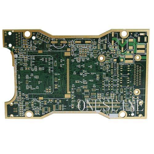
10 Layer HDI PCB High TG Fr4 Circuit Board One-stop Solutions
PCB details:
Material | Isola fr4 | Surface finish | ENIG |
Layer | 10 | Special | HDI PCB |
Thickness | 2.3MM | Copper | 1OZ |
Board size | 8*9CM | Solder mask | Green |
Silkscreen | White | Min line | 2mil |
Min hole | 3mil | Laser line | yes |
Buried hole | yes | Blind hole | yes |
Specializing in advanced 10-layer HDI (High Density Interconnect) PCBs fabricated on High Tg FR4 laminate, providing comprehensive one-stop solutions. Our expertise encompasses the complex design, precision manufacturing, and rigorous testing required for these sophisticated multilayer boards. Leveraging high Tg FR4 material ensures exceptional thermal reliability (typically Tg ≥ 170°C), critical for demanding applications involving lead-free assembly processes, high-power components, or harsh operating environments. The HDI technology, featuring microvias, fine line/space capabilities, and potentially sequential lamination, enables significant miniaturization and enhanced electrical performance essential for modern high-speed digital and RF designs. Our full-service approach integrates design for manufacturability (DFM) analysis, advanced fabrication utilizing laser drilling and precise plating, stringent quality control including electrical testing and AOI, and assembly support – delivering a complete, reliable turnkey solution for your mission-critical 10-layer HDI requirements.
Key Technical Points Highlighted:
10-Layer Complexity: Acknowledges the design and manufacturing challenges of a high layer count.
HDI Technology: Explicitly mentions core HDI features: microvias, fine lines/spaces, and the potential need for sequential lamination. Highlights benefits: miniaturization & enhanced electrical performance.
High Tg FR4: Clearly states the base material and emphasizes its key advantage: high thermal reliability (Tg ≥ 170°C). Links this directly to applications needing it (lead-free assembly, high power, harsh environments).
Target Applications: Implied or mentioned: modern electronics, high-speed digital, RF, mission-critical systems, miniaturized devices.
One-Stop/Turnkey Solution: Emphasizes the full-service nature covering the entire lifecycle: Design (including DFM), Fabrication (specifying advanced processes like laser drilling), Testing (electrical test, AOI), and Assembly Support.
Quality & Reliability: Mentioned through rigorous testing, stringent quality control, and the inherent reliability of the chosen materials and processes.
Technical Terminology: Uses appropriate terms (laminate, microvias, sequential lamination, plating, AOI, electrical testing, DFM, turnkey) demonstrating expertise.
Categories
News
Contact Us
Contact: Flexible PCB
Phone: 0086 18682010757
E-mail: kico@oneseine.com
Add: BldB,Fushan Industrial Park,Qianwu Town,Doumen,Zhuhai,China
