PCB fabrication
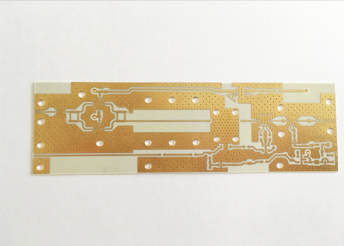
China Factory PCB Fast Prototyping Rogers Laminated Datasheet 4003C 0.2mm
China Factory PCB Fast Prototyping Rogers Laminated Datasheet 4003C 0.2mm
PCB Technology:
PCB Material: | Rogers 4003C | Product Name: | Rogers 4003 PCB Boards |
Layers: | 2 Layer | Copper | 1oz |
PCB Thickness: | 0.25mm | Surface | Immersion gold 1U tk |
Min. Line Width: | 0.1mm(4mil) | Min. Line Spacing: | 0.1mm(4mil) |
Min. Hole Size: | 0.15mm(6mil) | Rogers PCB: | Rogers 4003C pcb |
Soldermask | No | Silkscreen | No |
Rogers 4003C material selection:
Generally,4003 0.2MM/0.5MM/0.8MM are sufficient in our company,and the price will be cheaper than other thickness, the cheapest is 0.5MM thickness
For multilayer pcb boards,if you want to save costing and achieve the desired effect,I will suggest you use RO4003 material mix stack up Fr4 material,the main signal layer use rogers 4003 material and the other layer use fr4 material.
You can make some samples pcb prototype and test if it is OK
We have many many customers,their engineers design rogers +fr4 together, and have perfect result,the costing twice cheaper than rogers+rogers
And for single layer rogers 4003 PCB,if you think rogers 4003 exceed your budget, I think you can try to use china-made high frequency pcb material.F4B high frequency material,the DK have from 2.2-10,DF you can see here,if haven’t,can contact me directly.
Rogers 4003C application:
Automotive, Backplanes, RF / Microwave, High End Computing
Signal Integrity, Medical, Military, Mobile Devices / Wireless Handsets
Railway, Servers, Switches/Routers, Thermal Management, Wireless Infrastructure
Rogers High Frequency 4003 Material Laminate in stock
Rogers pcb material in stock:
Rogers4003C: thickness(0.2, 0.508,0.813,1.524) DK 3.38
Rogers4350B: thickness(0.168,0.254 0.508,0.762,1.524) DK 3.5
Rogers5880: thickness(0.254 ,0.508,0.762) DK 2.2
Rogers3003: thickness(0.127,0.508,0.762,1.524) DK 3
Rogers3010: thickness(0.635) DK 10.2
Rogers3206: thickness(0.635) DK 10.2
Rogers3035: thickness(0.508) DK 3.5
Rogers6010: thickness(0.635,1.27) DK 10.2
Materials used for HF circuit boards
Based on a variety of parameters, HF signals are reflected on circuit board, meaning that the impedance (dynamic resistance) varies with respect towards the sending component. To prevent such capacitive effects, all parameters must be exactly specified, and implemented with the highest amount of approach manage.
Vital for the impedances in high frequency printed circuit boards are principally the conductor trace geometry, the layer buildup, along with the dielectric continuous (er) on the supplies applied.
For many applications, it is sufficient to use Rogersmaterial with an appropriate layer buildup. In addition, we process high-frequency materials with improved dielectric properties. These have a very low loss factor, a low dielectric constant, and are primarily temperature and frequency independent.
Additional favourable properties are high glass transition temperature, an excellent thermal durability, and very low hydrophilic rate.
We use (among others) Rogers or PTFE materials (for example, Teflon from DuPont) for impedance controlled high frequency circuit boards. Sandwich buildups for material combinations are also possible.
The increasing complexity of electronic components and switches continually requires faster signal flow rates, and thus higher transmission frequencies. Because of short pulse rise times in electronic components, it has also become necessary for high frequency (HF) technology to view conductor widths as an electronic component.
Categories
News
Contact Us
Contact: Flexible PCB
Phone: 0086 18682010757
E-mail: kico@oneseine.com
Add: Building9,Xinyuan Industrial Park,Tangwei,Fuyong,Baoan,Shenzhen,China


