Special FPC
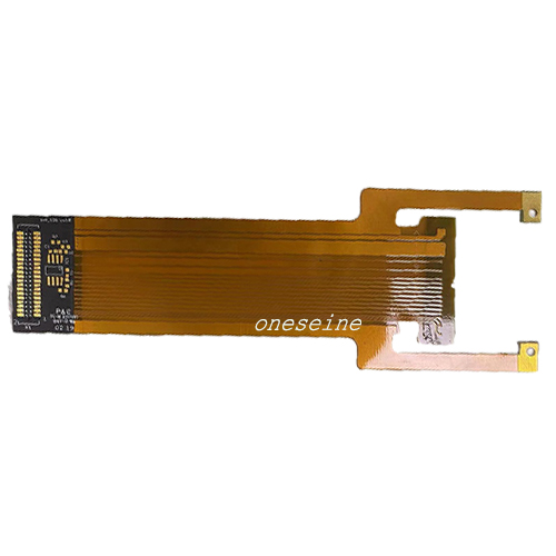
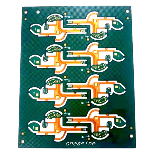
Rigid Flexible Fr4 PCB Manufacturing With Through-Hole For Commercial Plant
Rigid Flexible Fr4 PCB Manufacturing With Through-Hole For Commercial Plant
PCB parameter:
Number of layers: 4
Brand:Oneseine
Material: Polymide
Minimum line width/line spacing: 0.1mm
Copper thickness: 1OZ
Surface technology: ENIG
Solder resistance: Green for rigid part,yellow for flex part
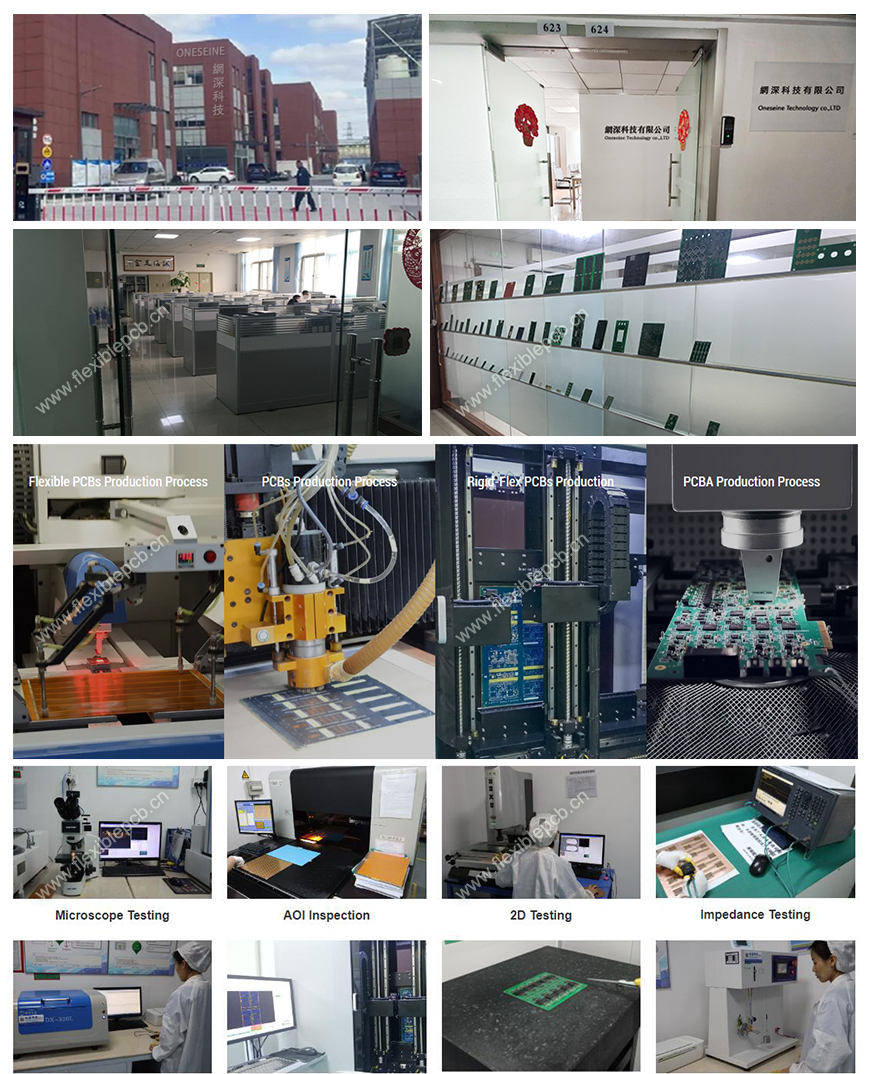
Oneseine Flexible PCB & Rigid-Flex PCB Process Capability
| Category | Process Capability | Category | Process Capability |
| Production Type | Single layer FPC / Double layers FPC Multi-layer FPC / Aluminum PCBs Rigid-Flex PCB | Layers Number | 1-30 layers FPC 2-32 layers Rigid-FlexPCB 1-60 layers Rigid PCB HDI Boards |
| Max Manufacture Size | Single layer FPC 4000mm Double layers FPC 1200mm Multi-layers FPC 750mm Rigid-Flex PCB 750mm | Insulating Layer Thickness | 27.5um /37.5/ 50um /65/ 75um / 100um / 125um / 150um |
| Board Thickness | FPC 0.06mm - 0.4mm Rigid-Flex PCB 0.25 - 6.0mm | Tolerance of PTH Size | ±0.075mm |
| Surface Finish | Immersion Gold/Immersion Silver/Gold Plating/Tin Plating/OSP | Stiffener | FR4 / PI / PET / SUS / PSA/Alu |
| Semicircle Orifice Size | Min 0.4mm | Min Line Space/ width | 0.045mm/0.045mm |
| Thickness Tolerance | ±0.03mm | Impedance | 50Ω-120Ω |
| Copper Foil Thickness | 9um/12um / 18um / 35um 70um/100um | Impedance Controlled Tolerance | ±10% |
Tolerance of NPTH Size | ±0.05mm | The Min Flush Width | 0.80mm |
| Min Via Hole | 0.1mm | Implement Standard | GB / IPC-650 / IPC-6012 / IPC-6013II / IPC-6013III |
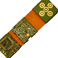
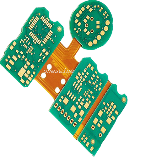
Advantage of FPCs
Potential to replace multiple rigid boards and/or connectors
Single-Sided circuits are ideal for dynamic or high-flex applications
Stacked FPCs in various configurations
Disadvantages of FPCs
Cost increase over rigid PCBs
Increased risk of damage during handling or use
More difficult assembly process
Repair and rework is difficult or impossible
Generally worse panel utilization resulting in increased cost
FPC Manufacturing
Flexible printed circuits (FPC) are made with a photolithographic technology. An alternative way of making flexible foil circuits or flexible flat cables (FFCs) is laminating very thin (0.07 mm) copper strips in between two layers of PET. These PET layers, typically 0.05 mm thick, are coated with an adhesive which is thermosetting, and will be activated during the lamination process. FPCs and FFCs have several advantages in many applications:
Tightly assembled electronic packages, where electrical connections are required in 3 axes, such as cameras (static application).
Electrical connections where the assembly is required to flex during its normal use, such as folding cell phones (dynamic application).
Electrical connections between sub-assemblies to replace wire harnesses, which are heavier and bulkier, such as in cars, rockets and satellites.
Electrical connections where board thickness or space constraints are driving factors.
Polyimide is a widely used flexible substrate material for flex circuit prototyping and manufacturing, and it offers several key advantages:
oneseine
1. Superior Flexibility and Durability:
- Polyimide has excellent flexibility, allowing it to withstand repeated bending and flexing without cracking or breaking.
- It has a high resistance to fatigue, making polyimide-based flex circuits suitable for applications with dynamic flexing requirements.
2. Thermal Stability:
- Polyimide has a high glass transition temperature (Tg) and can operate at elevated temperatures, typically up to 260°C.
- This thermal stability makes polyimide suitable for applications with high-temperature environments or processes, such as soldering.
3. Excellent Electrical Properties:
- Polyimide has a low dielectric constant and dissipation factor, which helps maintain signal integrity and minimizes crosstalk in high-frequency applications.
- It also exhibits high insulation resistance and dielectric strength, enabling the use of fine-pitch traces and high-density circuits.
4. Chemical and Environmental Resistance:
- Polyimide is highly resistant to a wide range of chemicals, solvents, and environmental factors, such as moisture and UV exposure.
- This resistance makes polyimide-based flex circuits suitable for applications in harsh environments or where they may be exposed to various chemicals.
5. Dimensional Stability:
- Polyimide has a low coefficient of thermal expansion (CTE), which helps maintain dimensional stability and minimize distortion during fabrication and assembly.
- This property is particularly important for achieving high-precision, high-density circuits.
6. Availability and Customization:
- Polyimide-based flex circuit materials are widely available from various suppliers, making them accessible for prototyping and production.
- These materials can also be customized in terms of thickness, copper foil weight, and other specifications to meet specific design requirements.
The combination of superior mechanical, thermal, electrical, and environmental properties makes polyimide an excellent choice for flex circuit prototyping and production, particularly for applications that require high reliability, flexibility, and performance.
Here's an overview of the flex PCB manufacturing process and some of the key challenges involved:
1. Design and Preparation:
- Flex PCB design considerations, such as trace/space requirements, via placement, and rigid-flex integration.
- Creation of detailed design files, including Gerber data, bill of materials, and assembly drawings.
- Selection of appropriate flexible substrate materials (e.g., polyimide, polyester) based on the application requirements.
2. Photolithography and Etching:
- Application of photoresist on the flexible substrate.
- Exposure and development of the photoresist to create the desired circuit pattern.
- Copper etching to remove unwanted copper and form the circuit traces.
- Challenges: Maintaining dimensional accuracy and avoiding undercut during etching.
3. Plating and Finishing:
- Electroplating of the copper traces to increase thickness and improve conductivity.
- Application of surface finishes, such as ENIG (Electroless Nickel Immersion Gold) or HASL (Hot Air Solder Leveling).
- Challenges: Ensuring uniform plating and avoiding defects or discoloration.
4. Multilayer Construction (if applicable):
- Lamination of multiple flexible layers with conductive and dielectric materials.
- Drilling and plating of vias to establish electrical connections between layers.
- Challenges: Controlling registration and alignment between layers, managing layer-to-layer insulation.
5. Cutting and Shaping:
- Precise cutting and shaping of the flex PCB using techniques like laser cutting or die-cutting.
- Challenges: Maintaining dimensional accuracy, avoiding material deformation, and ensuring clean cuts.
6. Assembly and Testing:
- Placement of electronic components on the flex PCB using techniques like surface mount or integrated assembly.
- Electrical testing to ensure the integrity of the circuit and compliance with design specifications.
- Challenges: Handling the flexibility of the substrate during assembly, maintaining solder joint reliability, and performing accurate testing.
7. Packaging and Protective Measures:
- Application of protective coatings, encapsulation, or stiffeners to enhance the durability and reliability of the flex PCB.
- Challenges: Ensuring compatibility between the protective measures and the flex PCB materials, maintaining flexibility, and avoiding delamination.
Key Challenges in Flex PCB Manufacturing:
- Maintaining dimensional accuracy and avoiding distortion during the fabrication process
- Ensuring reliable electrical connections and minimizing signal integrity issues
- Addressing adhesion and delamination concerns between layers and components
- Handling the flexibility and fragility of the substrate during various manufacturing stages
- Optimizing the manufacturing process to achieve high yields and consistent quality
Overcoming these challenges requires specialized equipment, processes, and expertise in flex PCB design and manufacturing. Collaboration with experienced flex circuit manufacturers can help navigate these complexities and ensure the successful production of reliable, high-performance flex PCBs.
News
Contact Us
Contact: Flexible PCB
Phone: 0086 18682010757
E-mail: kico@oneseine.com
Add: BldB,Fushan Industrial Park,Qianwu Town,Doumen,Zhuhai,China
