PCB fabrication
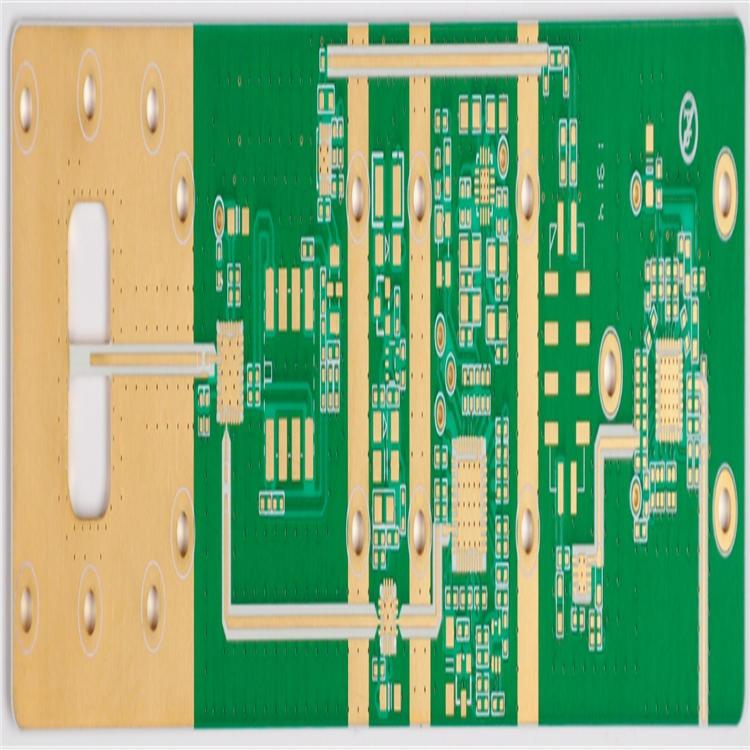
Rogers & Arlon AD350A High-Frequency PCB | 2.228mm 2-Layer ENIG Prototype Fabrication
Rogers & Arlon AD350A High-Frequency PCB | 2.228mm 2-Layer ENIG Prototype Fabrication
High-frequency and microwave applications demand PCB materials with tightly controlled dielectric properties, low signal loss, and stable performance across frequency and temperature. Two of the most trusted material families in this domain are Rogers high-frequency laminates and Arlon AD350A — both engineered for RF, microwave, and high-speed digital designs where standard FR-4 simply cannot meet the performance requirements.
This article details the technical specifications, material characteristics, manufacturing considerations, and application context of a 2-layer, 2.228mm-thick high-frequency PCB prototype built on Rogers / Arlon AD350A material with ENIG surface finish.
1. Product Specifications
This high-frequency PCB prototype is designed for RF and microwave applications requiring precise impedance control and low insertion loss. The key specifications are:
Product Type: Rogers high-frequency PCB prototype (also available in Arlon AD350A material)
Board Size: 18cm × 6cm (180mm × 60mm)
Surface Finish: ENIG (Electroless Nickel Immersion Gold)
Board Thickness: 2.228mm
Layer Count: 2 layers (double-sided)
Solder Mask: Green
Silkscreen (Legend): White
Material Options: Rogers high-frequency laminate or Arlon AD350A
2. Rogers High-Frequency Laminates: An Overview
Rogers Corporation is a leading manufacturer of high-frequency PCB materials, offering a broad portfolio of ceramic-filled PTFE and hydrocarbon ceramic laminates. Each Rogers material is engineered for specific frequency ranges, dielectric constants, and loss requirements.
2.1 Common Rogers Material Families
RO4000® Series (RO4003C, RO4350B, RO4360, RO4533, RO4535): Hydrocarbon ceramic laminates designed for high-volume commercial RF and microwave applications. RO4350B (Dk 3.48, Df 0.0037 at 10GHz) is the industry workhorse for power amplifiers, antennas, and automotive radar.
RO3000® Series (RO3003, RO3006, RO3010, RO3203, RO3206, RO3210): PTFE-based laminates with tightly controlled dielectric constants from 3.0 to 10.2, used for high-performance RF, microwave, and millimeter-wave circuits.
RO5880™ / RO5870™: Pure PTFE-glass laminates with ultra-low loss (Dk 2.2, Df 0.0009 at 10GHz for RO5880), ideal for millimeter-wave and ultra-high-frequency designs.
RO6000® Series: Laminates designed for automotive radar and high-volume millimeter-wave applications.
2.2 Key Advantages of Rogers Materials
Low dielectric loss (Df): Minimizes signal attenuation and heat generation — critical for high-power RF amplifiers and sensitive receiver circuits
Tightly controlled dielectric constant (Dk): Ensures consistent and predictable impedance across the board and between production batches
Low moisture absorption: Maintains stable electrical properties in humid environments
Excellent thermal stability: Dk changes minimally over temperature, ensuring consistent circuit performance
Proven reliability: Widely qualified for automotive, aerospace, defense, and telecommunications applications
3. Arlon AD350A: A Closer Look
In addition to Rogers materials, this prototype is also available in Arlon AD350A — a high-performance glass-reinforced PTFE composite laminate from Arlon (now part of DuPont's electronic materials portfolio).
3.1 Arlon AD350A Key Properties
Dielectric Constant (Dk): Approximately 3.50 at 10GHz, tightly controlled across the panel and between batches
Dissipation Factor (Df): Approximately 0.003 at 10GHz — low loss for efficient RF signal transmission
Reinforcement: Woven glass fiber, providing excellent dimensional stability and mechanical rigidity
Resin System: PTFE (polytetrafluoroethylene) composite, offering superior high-frequency performance compared to hydrocarbon-based materials
Thermal Conductivity: Moderate thermal conductivity, suitable for medium-power RF circuits
CTE (Coefficient of Thermal Expansion): Low and stable, ensuring reliable plated through-holes and solder joint integrity over thermal cycling
3.2 Arlon AD350A vs. Rogers: When to Choose Which
Both Arlon AD350A and Rogers RO4000-series materials serve similar high-frequency applications, but there are subtle differences:
Arlon AD350A offers a Dk of approximately 3.50, sitting between Rogers RO4003C (Dk 3.38) and RO4350B (Dk 3.48), making it a good alternative when a specific Dk value is required
Arlon materials are often preferred in defense, aerospace, and high-reliability applications where long-standing material qualification and consistent supply are critical
Rogers materials offer a broader product portfolio with more Dk options and are widely used in commercial high-volume applications such as automotive radar and 5G infrastructure
Both materials require similar specialized processing (drilling, etching, lamination) compared to standard FR-4
4. The Significance of 2.228mm Board Thickness
The finished board thickness of 2.228mm is a precise, non-standard value that reflects a specific design requirement — most commonly related to impedance control or mechanical fit.
4.1 Impedance and Dielectric Thickness
For a 2-layer microstrip PCB (signal on top, ground plane on bottom), the characteristic impedance of a trace is determined by:
Trace width (wider trace = lower impedance)
Dielectric thickness (thicker dielectric = higher impedance)
Dielectric constant (Dk) (higher Dk = lower impedance)
Copper thickness (minor effect)
A 2.228mm dielectric thickness is relatively thick for a high-frequency board, which means that for a given target impedance (typically 50Ω for RF), the required trace width will be wider than on a thinner board. This can be advantageous for:
High-power RF circuits: Wider traces handle more current and dissipate heat better
Lower insertion loss: Wider traces have lower conductor loss
Mechanical robustness: A thicker board is stiffer and less prone to warpage
The precise 2.228mm value likely results from a specific laminate ply thickness plus copper weights — for example, a 2.2mm dielectric core plus 2×14μm (1/2oz) copper on each side, or a custom ply stack designed to hit an exact impedance target.
4.2 Mechanical Considerations
A 2.228mm-thick 2-layer board provides excellent mechanical rigidity for its 18×6cm size, reducing the risk of flex-induced cracks in traces or solder joints. This is particularly important for RF circuits where even minor dimensional changes can alter impedance and circuit performance.
5. ENIG Surface Finish for High-Frequency PCBs
ENIG (Electroless Nickel Immersion Gold) is the specified surface finish for this high-frequency prototype — and it is one of the most popular choices for RF and microwave PCBs.
5.1 How ENIG Works
ENIG is a two-layer metallic coating applied over the copper pads:
Electroless Nickel: A layer of nickel (typically 3–6μm / 120–240μin) is deposited via chemical reduction, providing a barrier layer that prevents copper migration and oxidation
Immersion Gold: A thin layer of gold (typically 0.05–0.15μm / 2–6μin) is deposited via displacement reaction, protecting the nickel from oxidation and providing a highly solderable, flat surface
5.2 Why ENIG Is Preferred for High-Frequency PCBs
Flat surface: ENIG provides a planar (coplanar) surface, essential for fine-pitch components, QFNs, BGAs, and surface-mount RF connectors — unlike HASL, which leaves an uneven, curved solder surface
Excellent solderability: The gold layer dissolves into the solder during reflow, forming a reliable nickel-tin intermetallic bond
Long shelf life: ENIG-finished boards typically have a shelf life of 12 months when properly stored, compared to 6–12 months for OSP and 6 months for immersion silver
Good conductivity at high frequencies: While the nickel layer is non-magnetic and has slightly higher RF loss than pure copper, the thin gold layer and the fact that most RF current flows in the copper (skin effect) make ENIG suitable for most RF applications up to several GHz
Multiple reflow cycles: ENIG withstands multiple reflow cycles without significant degradation, important for complex assemblies
Aluminum wire bonding compatibility: ENIG is suitable for aluminum wire bonding in certain hybrid microelectronic assemblies
5.3 ENIG Considerations
Black pad risk: Over-immersion of gold can cause corrosion of the nickel layer (known as "black pad" or "black nickel"), leading to brittle solder joints. A reputable manufacturer controls the immersion gold process to avoid this defect.
Cost: ENIG is more expensive than OSP or HASL, but its performance benefits justify the cost for high-frequency and fine-pitch applications.
Signal loss at very high frequencies: At millimeter-wave frequencies (above ~30GHz), the nickel layer's conductivity and magnetic properties can introduce additional insertion loss. For these extreme frequencies, designers may specify alternative finishes such as immersion silver (ImAg) or even bare copper (with appropriate handling).
6. 2-Layer High-Frequency PCB Design Considerations
A 2-layer (double-sided) high-frequency PCB is the simplest and most cost-effective configuration for many RF and microwave circuits.
6.1 Typical Layer Stackup for 2-Layer RF PCB
Top Layer: Signal layer — contains RF traces (microstrip lines), component pads, and possibly copper pour for grounding
Bottom Layer: Solid ground plane — provides a continuous return path for RF signals, shields against interference, and serves as a heat spreader
This microstrip configuration is the most common topology for 2-layer RF boards, as it allows easy access for probing, component placement, and tuning.
6.2 Critical Design Rules for 2-Layer High-Frequency PCBs
Continuous ground plane: The bottom layer must be a solid, uninterrupted ground plane. Any splits, gaps, or cutouts under RF traces create return-path discontinuities, causing impedance changes, radiation, and signal loss.
Via stitching: Ground vias should be placed along the edges of RF traces and around the board perimeter to tie the top-layer ground pour to the bottom ground plane, reducing radiation and improving isolation.
Impedance control: All RF traces (typically 50Ω, or 75Ω for video/CATV) must be precisely width-controlled based on the actual dielectric thickness, Dk, and copper thickness. The manufacturer should provide an impedance calculation or use a field solver to verify.
Trace routing: Avoid 90-degree corners (use 45-degree or curved bends), maintain consistent trace width, and keep RF traces away from board edges and digital signals.
Component placement: Place RF components close together to minimize trace length, and isolate high-power amplifier outputs from sensitive receiver inputs.
Solder mask over RF traces: In some high-frequency designs, solder mask over microstrip traces can slightly alter impedance and increase loss. Designers may specify "solder mask defined" (SMD) or "non-solder mask defined" (NSMD) pads, and optionally request no solder mask over critical RF traces.
7. Green Solder Mask and White Silkscreen
Green solder mask: Green is the most common and cost-effective solder mask color. It provides good contrast for visual inspection, is widely available from all solder mask suppliers, and has well-characterized electrical and thermal properties. For high-frequency boards, the solder mask's dielectric properties (Dk ~3.0–3.5, Df ~0.02) can slightly affect trace impedance if applied over RF lines — this should be accounted for in impedance calculations.
White silkscreen: White legend ink provides high contrast against the green solder mask, making component designators, polarity marks, and logos clearly visible for assembly, inspection, and rework. Silkscreen should never be placed on RF pads, fine-pitch component pads, or critical RF traces, as it can interfere with soldering and signal performance.
8. Prototype Fabrication for High-Frequency PCBs
High-frequency PCB prototypes require specialized manufacturing capabilities beyond standard FR-4 production:
8.1 Material Handling and Storage
Rogers and Arlon PTFE-based materials are moisture-sensitive and should be stored in dry cabinets or vacuum-sealed packaging with desiccant
Materials must be brought to room temperature before opening to prevent condensation
Material shelf life and lot traceability must be maintained to ensure consistent electrical properties
8.2 Specialized Processing
Drilling: PTFE-based materials require specialized drill parameters (slower feed rates, optimized drill bit geometry, and frequent bit changes) to prevent hole wall smearing and resin pullback
Etching: High-frequency materials may use different copper foil treatments (e.g., reverse-treated foil for low profile), requiring adjusted etching parameters to achieve target line width
Solder mask: Specialized solder mask materials and curing profiles may be required for proper adhesion to Rogers/Arlon substrates
Impedance verification: TDR (Time Domain Reflectometry) testing on test coupons or actual traces to verify that the fabricated impedance matches the design target
8.3 Quality Control for High-Frequency Prototypes
Dimensional inspection: Verify board thickness (2.228mm), trace width, and hole sizes
Impedance testing: TDR measurement of critical RF traces
Solderability test: Verify ENIG pad solderability per IPC-J-STD-003
AOI (Automated Optical Inspection): Detect shorts, opens, and registration errors
Microsection analysis: Verify copper thickness, hole wall quality, and layer alignment (for multi-layer; for 2-layer, verify plating and etch quality)
9. Typical Applications for This Type of High-Frequency PCB
A 2-layer, 2.228mm Rogers/Arlon AD350A PCB with ENIG finish is well-suited for:
RF power amplifiers (PA modules for cellular base stations, radar, or industrial RF)
Microstrip antennas and antenna feed networks
RF filters and couplers (low-pass, high-pass, band-pass, directional couplers)
LNA (Low-Noise Amplifier) circuits for receiver front-ends
Microwave sensor modules (motion detection, level measurement, speed sensing)
5G and mmWave test fixtures and evaluation boards
Automotive radar modules (24GHz, 77GHz)
Aerospace and defense RF subsystems
Satellite communication components
10. Conclusion
A 2-layer, 2.228mm-thick high-frequency PCB prototype built on Rogers or Arlon AD350A material with ENIG surface finish represents a focused, high-performance solution for RF and microwave applications. The combination of low-loss PTFE-composite substrate, precise dielectric thickness for controlled impedance, flat ENIG finish for reliable fine-pitch assembly, and a simple 2-layer microstrip stackup makes this board type ideal for RF prototypes, power amplifiers, filters, antennas, and sensor modules.
Both Rogers and Arlon AD350A offer tightly controlled dielectric constants, low dissipation factors, and excellent thermal stability — properties that are essential for predictable high-frequency circuit performance. When selecting a manufacturer for this type of prototype, it is critical to choose a fabricator with proven experience processing PTFE-based high-frequency materials, capable of drilling, etching, and impedance control to the tight tolerances that RF circuits demand.
Whether the project calls for Rogers or Arlon AD350A, the key to a successful high-frequency prototype lies in accurate impedance modeling, careful material handling, specialized processing, and rigorous quality verification — all of which a qualified Chinese PCB manufacturer can provide.
SEO Keywords
Rogers high frequency PCB, Arlon AD350A PCB, 2.228mm PCB, 2 layer RF PCB, ENIG surface finish PCB, Rogers PCB prototype, Arlon PCB fabrication, PTFE high frequency laminate, microstrip PCB 50 ohm, RF amplifier PCB, microwave PCB China, low loss PCB material, Rogers RO4350B prototype, high frequency PCB manufacturer, controlled impedance PCB prototype
Categories
News
Contact Us
Contact: Flexible PCB
Phone: 0086 18682010757
E-mail: kico@oneseine.com
Add: BldB,Fushan Industrial Park,Qianwu Town,Doumen,Zhuhai,China









