PCB fabrication
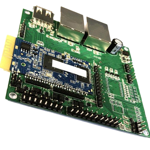
8 Layer HDI PCB FR4 Soldering Circuit Boards PCB PCBA Gold Fingers
8 Layer HDI PCB FR4 Soldering Circuit Boards PCB PCBA Gold Fingers
General information:
Layer:8
Material:Fr4
Board thickness:1.0mm
Copper weight:1OZ
Solder mask:Green
White silkscreen:White
Min line:5mil
Min hole:0.3mm
Name:SMT / DIP PCBA Assembly Control Circuit Boards
Application:Computer,communication field
PCB Assembly Concept:
PCBA is the abbreviation of Printed Circuit Board + Assembly, that is to say, the PCB bare board through the SMT, and then through the whole process of the DIP plug-in, referred to as the PCBA, which is commonly used in China, and the standard in Europe and America is PCB 'A, is added to the ramp point. This is called the official idiom, we communicate with foreign customers or when the promotion, they often ask what is PCBA.
A printed circuit board (PCB) mechanically supports and electrically connects electronic components using conductive tracks, pads and other features etched from copper sheets laminated onto a non-conductive substrate. Components – capacitors, resistors or active devices – are generally soldered on the PCB. Advanced PCBs may contain components embedded in the substrate.
PCBs can be single sided (one copper layer), double sided (two copper layers) or multi-layer (outer and inner layers). Conductors on different layers are connected with vias. Multi-layer PCBs allow for much higher component density.
FR-4 glass epoxy is the primary insulating substrate. A basic building block of the PCB is an FR-4 panel with a thin layer of copper foil laminated to one or both sides. In multi-layer boards multiple layers of material are laminated together.
Printed circuit boards are used in all but the simplest electronic products. Alternatives to PCBs include wire wrap and point-to-point construction. PCBs require the additional design effort to lay out the circuit, but manufacturing and assembly can be automated. Manufacturing circuits with PCBs is cheaper and faster than with other wiring methods as components are mounted and wired with one single part.
A minimal PCB with a single component used for easier modeling is called breakout board.
SMT / DIP PCBA control circuit boards Manufacturer
a) Components sourcing
Common components are replaced to be High Quality China brand componnets at the condition of permission,
Decreasing cost for clients is one part of our jobs.
Genuine components are ordered from your designated supplier or our partner companies including Digikey,Mouser,
Arrow, Avnet,Future Electronic,Farnell,etc.
b) Type of assembly
SMT and Thru-hole
c) Assembly capacity
Stencil size/range : 736 × 736mm
Minimum IC pitch : 0.30mm
Maximum PCB size : 410 × 360mm
Minimum PCB thickness : 0.35mm
Minimum chip size : 0201 (0.2 × 0.1)/0603 (0.6 x 0.3mm)
Maximum BGA size : 74 × 74mm
BGA ball pitch : 1.00mm (minimum), 3.00mm (maximum)
BGA ball diameter : 0.40mm (minimum), 1.00mm (maximum)
QFP lead pitch : 0.38mm (minimum), 2.54mm (maximum)
Frequency of stencil cleaning : 1 time/5 to 10 pieces
Categories
News
Contact Us
Contact: Flexible PCB
Phone: 0086 18682010757
E-mail: kico@oneseine.com
Add: Building9,Xinyuan Industrial Park,Tangwei,Fuyong,Baoan,Shenzhen,China


