Rigid-flex FPC
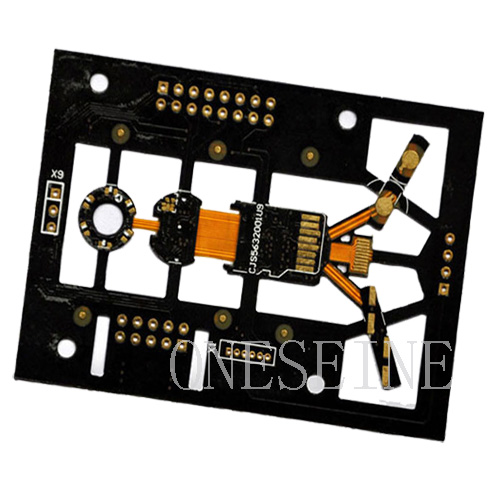
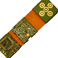
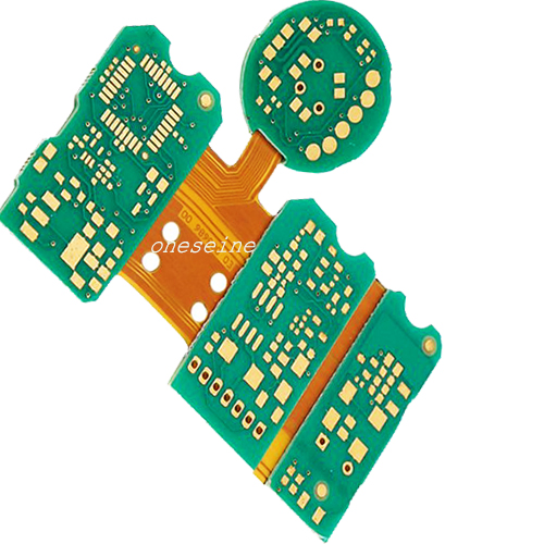
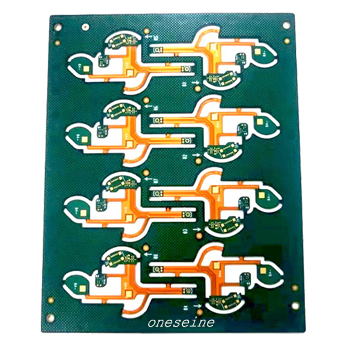
4L Rigid-flex Printed Circuit Boards 1.0MM PCB Thickness
4L Rigid-flex Printed Circuit Boards 1.0MM PCB Thickness
Quick detail:
Layer | 4 | Impedance | Yes |
Rigid part | Fr4 | Thickness | 0.6mm |
Flex part | Polyimide | Size | 1.72*7.76CM |
Copper | 1OZ | Surface finish | ENIG |
Soldermask | Green | Silkscreen | White |
Manufacturing Capacities of Flex Rigid PCB:
No. | Item | Description |
1 | Layer | Flex pcb: 1-6Layers |
Flex-Rigid pcb: 2-8Layers | ||
2 | Material | CCL, PI, PET, PEN, FR-4 |
3 | Final Thickness | Flex board: 0.002" - 0.1" (0.05-2.5mm) |
Flex-rigid board: 0.0024" - 0.16" (0.06-4.0mm) | ||
4 | Surface Treatment | Lead-free: ENG Gold, OSP, Immersion Silver, Immersion Tin |
5 | Min Trace | Inner: 0.5oz: 4/4mil Outer: 1/3oz-0.5oz: 4/4mil |
6 | Min Width /Clearance | 1oz: 5/5mil 1oz: 5/5mil |
2oz: 5/7mil 2oz: 5/7mil | ||
7 | Min Hole Ring | Inner: 0.5oz: 4mil Outer: 1/3oz-0.5oz: 4mil |
1oz: 5mil 1oz: 5mil | ||
2oz: 7mil 2oz: 7mil | ||
8 | Copper Thickness | 1/3oz - 2oz |
9 | Max / Min Insulation Thickness | 2mil/0.5mil (50μm/12.7μm) |
10 | Min Hole Size and Tolerance | Min Hole: 8mil |
Tolerance: PTH±3mil, NPTH±2mil | ||
11 | Min Slot | 24mil x 35mil (0.6x0.9mm) |
12 | Solder Mask Alignment Tolerance | ±3mil |
13 | Silkscreen Alignment Tolerance | ±6mil |
14 | Silkscreen Line Width | 5mil |
15 | Gold Plating | Nickel: 100μ" - 200μ" Gold: 1μ"-4μ" |
16 | Immersion Nickel / Gold | Nickel: 100μ" - 200μ" Gold: 1μ"-5μ" |
17 | Immersion Silver | Silver: 6μ" - 12μ" |
18 | OSP | Film: 8μ" - 20μ" |
19 | Test Voltage | Testing Fixture: 50-300V |
20 | Profile Tolerance of Punch | Accurate mould: ±2mil |
Ordinary mould: ±4mil | ||
Knife mould: ±8mil | ||
Hand-Cut: ±15mil |
Here are some tips for flex circuit prototyping:
Materials and Equipment Needed:
- Flexible circuit materials (e.g. polyimide, polyester, or polyethylene terephthalate (PET) films)
- Copper foil for conductive traces
- Photo-resist materials and UV exposure unit for etching
- Cutting tools (e.g. scissors, knife, laser cutter)
- Soldering iron and solder
- Adhesives and lamination equipment
Flex Circuit Design Considerations:
- Route traces to minimize bending stresses
- Provide strain relief for component attachment points
- Consider thermal expansion differences between materials
- Design for flexibility - minimize rigid areas
Flex Circuit Fabrication Process:
1. Start with a flexible base material and apply copper foil.
2. Apply and expose photo-resist to define trace patterns.
3. Chemically etch away unwanted copper.
4. Remove remaining photo-resist.
5. Optional: Apply solder mask and surface finish.
6. Cut the flexible circuit to shape using cutting tools.
7. Assemble and attach components using soldering or adhesives.
Prototyping Tips:
- Start with simple, single-layer designs to test your process.
- Experiment with different flexible base materials and thicknesses.
- Utilize laser cutting or other precision tools for complex shapes.
- Test bend radius and flexing performance during development.
- Consult flex circuit design guidelines and seek expert advice as needed.
The key to successful flex circuit prototyping is taking an iterative, hands-on approach to learn the process and optimize the design for your specific application. Let me know if you have any other questions!
Here is an example of a typical flex circuit fabrication workflow you can follow for prototyping:
Step 1: Design the Flex Circuit
- Use CAD software to create the flex circuit layout, including trace routing, component placement, and overall shape.
- Ensure the design accounts for flexibility requirements, such as bend radii and strain relief.
- Export the design files in a format suitable for fabrication, such as Gerber files.
Step 2: Prepare the Flexible Substrate
- Select an appropriate flexible base material, such as polyimide or polyester film.
- Clean the substrate surface to promote good adhesion.
- Apply a copper foil layer to the flexible substrate, either through lamination or direct deposition.
Step 3: Apply Photoresist and Expose the Trace Pattern
- Coat the copper-clad substrate with a light-sensitive photoresist material.
- Use a UV exposure unit and the Gerber files to selectively expose the desired trace pattern on the photoresist.
- Develop the photoresist to remove the unexposed areas, leaving the copper traces protected.
Step 4: Etch the Copper Traces
- Place the developed substrate in a chemical etchant solution to remove the exposed copper.
- Carefully monitor the etching process to ensure the desired trace pattern is achieved.
- Clean the substrate and remove the remaining photoresist.
Step 5: Add Optional Layers (Solder Mask, Surface Finish)
- If desired, apply a solder mask layer to protect the copper traces.
- Consider adding a surface finish, such as electroplated gold or tin, to enhance solderability.
Step 6: Cut and Shape the Flex Circuit
- Use a cutting tool, such as a laser cutter or precision knife, to cut the flex circuit to the desired shape and size.
- Ensure the cutting process does not damage the copper traces or the flexible substrate.
Step 7: Assemble and Test the Flex Circuit
- Solder or attach components to the flex circuit using appropriate adhesives or interconnection methods.
- Thoroughly test the flex circuit, including flexibility testing, to ensure it meets the design requirements.
- Iterate on the design and fabrication process as needed to optimize the flex circuit performance.
This is a general workflow, and the specific steps may vary depending on the flex circuit complexity, available equipment, and your experience level. Remember to consult flex circuit design guidelines and seek expert advice as needed throughout the prototyping process.
News
Contact Us
Contact: Flexible PCB
Phone: 0086 18682010757
E-mail: kico@oneseine.com
Add: Building9,Xinyuan Industrial Park,Tangwei,Fuyong,Baoan,Shenzhen,China


