PCB fabrication
Multi-Layer HDI PCB Maker Near Me Circuit Boards Quick Turn Pcb Manufacturers
Multi-Layer HDI PCB Maker Near Me Circuit Boards Quick Turn Pcb Manufacturers
Quick detail:
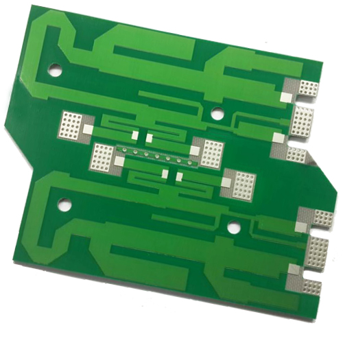
Layer:4
Board material:Fr4
Surface finish:HASL lead free
Copper weight:1OZ
Board thickness:1.6mm
PCB assembly:yes
Solder mask:Green
Silkscreen:White
Product name:4 Layer PCB assembly prototype
Multi-Layer HDI PCB Maker Near Me Circuit Boards Quick Turn Pcb Manufacturers
PCBS Printed Circuit Boards Manufacturers
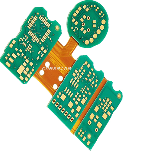
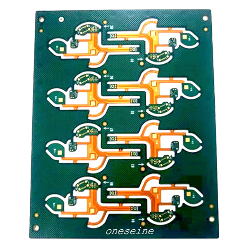
The name of circuit board: circuit boards, PCB board, aluminum board, high frequency board, thick copper board, impedance board,ultra-thin circuit boards, printing (copper etching technology) circuit boards. Circuit board made the circuit mini, intuitive, for the fixed-circuit production and optimization of electrical layout plays an important role. (Printed Circuit Board) PCB (Flexible Printed Circuit board) FPC circuit board (FPC circuit board, also known as flexible circuit board Flexible circuit board is a poly High reliability, excellent flexible printed circuit board with high wiring density, light weight, thin thickness, good bending characteristics! And flex and rigid combination plate (reechas, Soft and hard combination plate) -FPC and PCB birth and development, gave birth to the flex and rigid combination board this new product. Therefore, the flex and rigid combination board, is a flexible circuit board and rigid circuit board, through the pressure and other processes, according to the relevant process requirements together to form a FPC characteristics and PCB characteristics of the circuit board.
The types of circuit board
Board divided by the number of layers, cab be single sided pcb, double sided pcb, and multi-layer pcb circuit board
First, the single-sided PCB, in the most basic PCB, the parts concentrated in one side, the wire is concentrated in the other side. Because the wire only appears in one side, so called the PCB called single-sided circuit board. Single-sided panels are usually made simple, low cost, but the shortcomings can not be applied to too complex products.
Double-sided panel is a single-panel extension, when the single-layer wiring can not meet the needs of electronic products, it is necessary to use the double panel. Both sides are covered with copper traces, and can be through the hole to turn between the two layers of the line, so that the formation of the required network connection.
A multilayer board is a printed circuit board having three or more conductive pattern layers interposed therebetween with insulating material interposed therebetween, and in which the conductive patterns are interconnected as required. Multi-layer circuit board is the electronic information technology to high-speed, multi-function, large capacity, small size, thin, lightweight direction of the product.
According to the characteristics of the circuit board, then divided into flexible pcb board (FPC), rigid pcb board (PCB), flex and rigid combination board (FPCB).
PCB Introduction:
A printed circuit board (PCB) mechanically supports and electrically connects electronic components using conductive tracks, pads and other features etched from copper sheets laminated onto a non-conductive substrate. Components – capacitors, resistors or active devices – are generally soldered on the PCB. Advanced PCBs may contain components embedded in the substrate.
PCBs can be single sided (one copper layer), double sided (two copper layers) or multi-layer (outer and inner layers). Conductors on different layers are connected with vias. Multi-layer PCBs allow for much higher component density.
FR-4 glass epoxy is the primary insulating substrate. A basic building block of the PCB is an FR-4 panel with a thin layer of copper foil laminated to one or both sides. In multi-layer boards multiple layers of material are laminated together.
Printed circuit boards are used in all but the simplest electronic products. Alternatives to PCBs include wire wrap and point-to-point construction. PCBs require the additional design effort to lay out the circuit, but manufacturing and assembly can be automated. Manufacturing circuits with PCBs is cheaper and faster than with other wiring methods as components are mounted and wired with one single part. Furthermore, operator wiring errors are eliminated.
When the board has no embedded components it is more correctly called a printed wiring board (PWB) or etched wiring board. However, the term printed wiring board has fallen into disuse. A PCB populated with electronic components is called a printed circuit assembly (PCA), printed circuit board assembly orPCB assembly (PCBA). The IPC preferred term for assembled boards is circuit card assembly (CCA), and for assembled backplanes it is backplane assemblies. The term PCB is used informally both for bare and assembled boards.
PCB process:
Double Sided HASL pcb board / immersion gold board Production process:
Shape cutting -----Drilling-----PTH -----Circuit -----Figure electric -----Etching----Solder mask----Silk screen-----HASL(ENIG)----Routing-----V-cut-----Testing----Vacuum packaging
Double Sided gold-plated pcb board production process:
Shape cutting----- Drilling -----PTH-----Circuit-----Figure electric-----Gold plated-----Etching-----Solder mask-----Silk screen-----Routing----V-cut-----Testing-----Vacuum packaging
Multi-layer PCB HASL / immersion gold PCB Production process:
Shape cutting---- Inner layer----Stack up----Drilling----PTH----Circuit----Circuit -----Figure electric -----Etching----Solder mask----Silk screen-----HASL(ENIG)----Routing-----V-cut-----Testing----Vacuum packaging
Multilayer plate gold plate production process:
Shape cutting----Inner layer----Stack up----Drilling----PTH----Circuit----Circuit -----Figure electric -----Etching----Solder mask----Silk screen-----HASL(ENIG)----Routing-----V-cut-----Testing----Vacuum packaging
Circuit Boards Composition:
Circuit board mainly by the pad, vias, mounting holes, wires, components, connectors,filler, Electrical boundary
Pad: A metal hole used to solder the pins of a component.
Through-hole: There are metal vias and non-metallic vias, in which the metal vias for connecting the components between the layers of the pin.
Mounting Holes: For securing the circuit board.
Wires: An electrical network copper foil used to connect the pins of a component.
Connectors: Components used for connection between circuit boards.
Filling: for the ground network of copper, can effectively reduce the impedance.
Electrical Boundary: Used to determine the size of the board, all the components on the circuit board can not exceed the boundary. .
Categories
News
Contact Us
Contact: Flexible PCB
Phone: 0086 18682010757
E-mail: kico@oneseine.com
Add: Building9,Xinyuan Industrial Park,Tangwei,Fuyong,Baoan,Shenzhen,China


